Vacuum coating technology is one of the major surface treatment techniques used in manufacturing. This technology supports everything from scratch-resistant phone screens to reflective surfaces on insulated bottles. By managing how materials deposit at the atomic level, it offers unique advantages depending on the material and purpose.
Fundamentals of Vacuum Coating Technology
Principles of Vacuum Deposition
Vacuum deposition forms thin films by converting a solid material into vapor and allowing it to condense on a substrate. The process occurs in a low-pressure environment that minimizes contamination and enables accurate control of film thickness and composition.
The vacuum environment reduces collisions between vapor particles and gas molecules, allowing the vapor to travel directly to the substrate. This improves coating uniformity and adhesion.
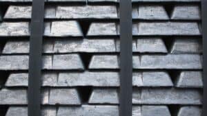
Common materials used include metals, ceramics, and compounds like titanium nitride or aluminum oxide. These coatings can enhance hardness, corrosion resistance, or optical properties depending on the application.
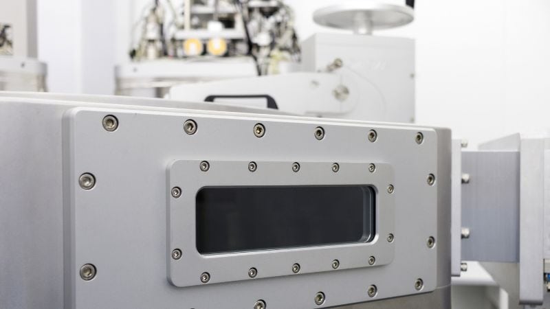
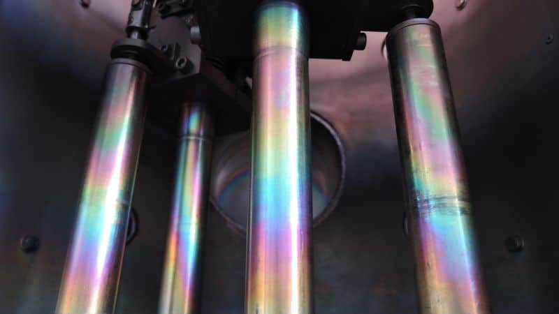
Components of the Vacuum Chamber
Importance of Substrate Selection
The substrate, which is the part that needs coating, acts as the foundation for the coating and strongly influences the film’s performance. Its composition, surface roughness, and thermal properties determine how well the coating adheres and functions.
Common substrates include glass, metal alloys, polymers, and ceramics. Each requires specific cleaning and preparation steps to remove oxides, oils, or particulates.
Surface treatments such as ion cleaning or plasma etching improve adhesion and create a stable interface. Careful substrate selection ensures that vacuum coatings meet durability, optical, or electrical requirements for their intended use.
PVD Vacuum Coating Processes
Physical Vapor Deposition (PVD) is a group of vacuum-based methods that create thin films by converting solid material into vapor and condensing it on a surface. This process utilizes heat, plasma, or electric fields to vaporize the source material, with sputtering and evaporation being the most common techniques. Both methods are renowned for providing strong adhesion and uniform thickness.
PVD coatings are applied to a variety of substrates, including metals, ceramics, and polymers. The technology offers several key advantages:
- High Film Purity: The vacuum environment prevents contamination.
- Strong Adhesion: Provides excellent bonding to metals and ceramics with proper surface pre-processing.
- Wide Temperature Range: Offers flexibility for various substrate materials.
- Low Environmental Impact: It is a solvent-free, dry process that avoids the harmful chemicals used in traditional wet plating.
As a result, PVD coatings provide high hardness, excellent corrosion resistance, and thermal stability. These properties make them ideal for demanding applications such as cutting tools, optical components, and electronic parts, positioning PVD as a cleaner and more environmentally friendly alternative.
Sputtering Techniques
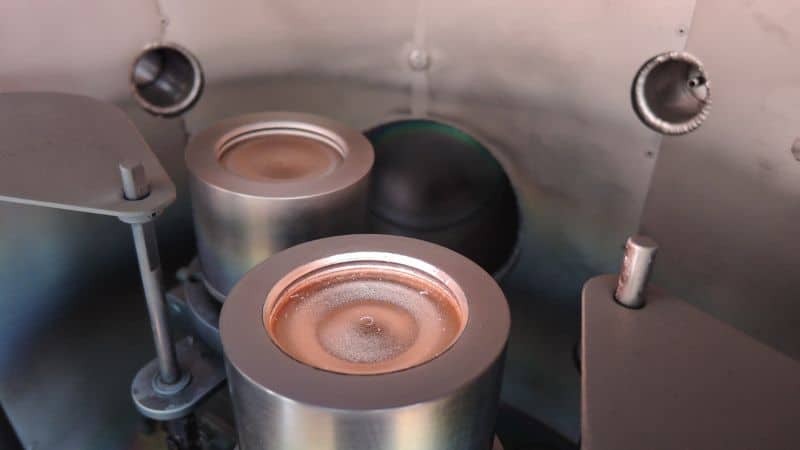
Sputtering is a PVD process where a device within the chamber uses ions to strike a solid target, causing its atoms to eject and deposit onto a substrate. It allows precise control of film thickness and composition.
The most common type is magnetron sputtering, which uses magnetic fields to trap electrons near the target surface. This increases efficiency while preventing excessive heating on the substrate. It works well for metals, oxides, and nitrides.
Sputtering produces dense, uniform coatings used in semiconductors, displays, and solar cells. It supports multi-layer structures and can coat complex shapes. Because it runs at lower temperatures than evaporation, it suits heat-sensitive materials like plastics or thin foils.
Evaporation Methods
Evaporation coating involves heating a material until it vaporizes and condenses on the substrate in a vacuum. The heat source may be resistive, electron beam, or arc-based, depending on the material’s melting point.
This method offers high deposition rates and produces smooth, uniform surfaces but requires careful temperature control to ensure consistent film quality.
Compared with sputtering, thermal evaporation can achieve faster coating speeds but may result in less dense films. It remains widely used for optical films, aluminum mirrors, semiconductor layers, and protective coatings where precise optical or electrical properties are needed.
CVD & ALD Vacuum Coating Techniques
Chemical Vapor Deposition (CVD)
Chemical Vapor Deposition (CVD) forms thin solid films through chemical reactions of materials inside a controlled chamber. Traditional thermal CVD often operates at high temperatures, allowing gases to react or decompose on a heated substrate surface. In addition, there are also plasma-enhanced (PECVD) and other variants that can operate at significantly lower temperatures.
CVD can produce high-purity, dense coatings with excellent adhesion. Its versatility makes it valuable in microelectronics, solar cells, and aerospace components, where precise and durable coatings are essential.
Atomic Layer Deposition (ALD)
Atomic Layer Deposition (ALD) builds thin films one atomic layer at a time through alternating exposure to precursor gases. Each reaction cycle deposits a controlled layer, ensuring exceptional thickness accuracy and conformal coverage even on complex 3D surfaces.
This precision allows ALD to create films only a few nanometers thick with uniformity across large substrates. It is widely used for semiconductor gate oxides, barrier layers, and protective coatings in flexible electronics and energy storage devices.
ALD operates at lower temperatures than traditional thermal CVD processes, making it compatible with heat-sensitive materials.
Its main strengths include:
- Angstrom-Level Thickness Control: Allows for deposition with atomic-scale precision.
- Excellent Step Coverage: Ensures uniform coatings even on complex 3D structures.
- Superior Material Properties: Produces high-quality dielectric and barrier films.
These traits make ALD a preferred method for next-generation nanocoatings and advanced device manufacturing.
Materials and Coatings in Vacuum Technology
Common Coating Materials
Vacuum coatings use metals, alloys, and compounds that can vaporize or sputter under vacuum. Common coating materials fall into two main categories:
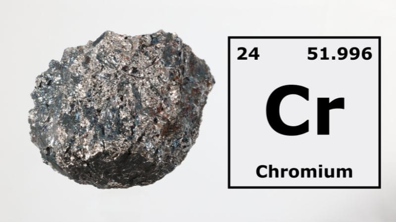
- Metals (e.g., Al, Ti, Cr, Au): Used for their reflective and conductive properties to improve durability and appearance.
- Ceramics & Compounds (e.g., TiN, Al₂O₃): Provide high hardness, wear resistance, and corrosion resistance for tools, optics, and functional parts.
These materials are deposited using physical vapor deposition (PVD) or chemical vapor deposition (CVD) methods, depending on the required film structure and performance.
Transparent Conductive Oxides (ITO)
Indium tin oxide (ITO) is one of the most important thin films in modern vacuum coating. It combines high optical transparency with electrical conductivity, making it essential for touchscreens, solar cells, and display panels.
ITO coatings are typically produced by magnetron sputtering under controlled vacuum conditions. The process allows precise control of film thickness and composition, which affects both transparency and resistance.
Because indium is relatively expensive and its supply is constrained, research continues into alternatives like aluminum-doped zinc oxide (AZO) and fluorine-doped tin oxide (FTO), which offer similar properties at a lower cost.
Nickel Oxide (NiO) and Specialized Films
Nickel oxide (NiO) is a multifunctional thin-film material used for electrochromic windows, sensors, and battery electrodes.
In vacuum coating, NiO films are often deposited by reactive sputtering or CVD, forming uniform layers on glass or metal substrates. The film’s optical and electrical behavior can be tuned by adjusting oxygen content during deposition.
Specialized coatings also include multilayer films that combine metals, oxides, or nitrides to achieve specific effects such as anti-reflection, thermal control, or magnetic recording. These films require precise layer thickness control, often within nanometers, to maintain consistent performance across large surfaces.
Applications and Industry Innovations
Electronics and Optics
In electronics and optics, vacuum coating creates essential functional layers. For electronics, it deposits conductive metallic and transparent oxide films for semiconductors, touchscreens, and various sensors.
In optical applications, the technology applies anti-reflective, reflective, and protective coatings on camera lenses, laser components, and solar panels to precisely control light transmission and reflection.
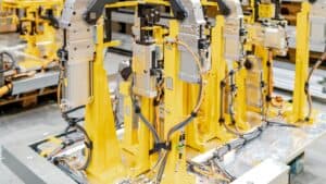
The latest industrial developments include advanced sputtering techniques like High-Power Impulse Magnetron Sputtering (HiPIMS) that produce denser films with fewer defects, along with AI-controlled monitoring systems that maintain consistent coating quality in high-volume production.
Automotive and Green Buildings
The automotive and construction industries benefit from vacuum coating’s durability and energy efficiency properties. Automotive manufacturers apply wear-resistant and decorative coatings to engine components, tools, and exterior trim, often as an environmentally friendly alternative to traditional electroplating.
In building construction, vacuum coating produces low-emissivity glass that reflects infrared heat while admitting visible light, significantly reducing heating and cooling energy requirements.
Technological advances in roll-to-roll coating enable cost-effective production of large, uniformly coated glass sheets and flexible films for architectural and automotive applications.
Additive Manufacturing and 3D Printing
Vacuum coating complements additive manufacturing by enhancing the surface properties of 3D printing components. The technology adds critical functionality to printed parts, including wear resistance to polymer prints and electrical conductivity to metal components. This capability allows 3D-printed prototypes and production parts to achieve performance characteristics similar to traditionally manufactured components, particularly valuable in aerospace, tooling, and electronic housing applications.
Medical and Industrial Tools
The medical and industrial sectors rely on vacuum coating for performance-critical applications. Medical device manufacturers use the technology to create biocompatible, antibacterial, and corrosion-resistant surfaces on implants and surgical instruments.
In industrial tooling, ultra-hard coatings such as titanium aluminum nitride (TiAlN) and chromium nitride (CrN) significantly extend tool life by reducing friction and wear during machining operations.
In modern industrial practices, automated, data-driven control systems also greatly contribute to the coating uniformity essential for precision medical instruments and industrial cutting tools.
Conclusion
As an advanced and complicated surface processing technique, vacuum coating allows manufacturers to create precise, durable, and clean coatings that improve performance across industries like electronics, automotive, aerospace, and medical devices. As a result, it has been integrated into the workflow of surface processing and many manufacturers provide vacuum coating service to their clients after manufacturing orders are complete.
Frequently Asked Questions
What are the limitations or challenges of vacuum coating?
The main challenges are the high capital cost and the size limitations imposed by the vacuum chamber. The process is also a “line-of-sight” technology for many PVD methods, meaning complex geometries with deep recesses or hidden areas can be difficult to coat uniformly without specialized fixturing and rotation.
Furthermore, achieving optimal adhesion requires meticulous and often expensive substrate cleaning and preparation.
Finally, the deposition rates, while sufficient for thin films, are much slower than traditional wet-coating processes like painting or plating, making it less suitable for very high-volume, low-value items.
How does the performance of PVD coating compare to traditional electroplating?
Compared to electroplating, PVD coatings generally offer superior performance in terms of hardness, wear resistance, and corrosion protection. They are typically denser, more uniform, and exhibit much better adhesion to the substrate.
From an environmental standpoint, PVD is a dry process that generates minimal hazardous waste, unlike electroplating, which relies on toxic chemical baths and produces significant liquid waste.
However, electroplating can be more cost-effective for simple, high-volume parts and is better at coating very complex internal surfaces.
